Understanding Failures to Better Correct Them
In the context of product development or production troubleshooting, electronic failures are not always visible or easily reproducible. A circuit may operate intermittently, exhibit unstable behavior, or fail for no apparent reason.
At Solutions Novika, our approach goes beyond traditional testing to identify the root causes of problems. We combine several complementary analysis techniques to gain a deep understanding of the phenomena at play.
A Multilevel Approach
In addition to its expertise and equipment in electromagnetic compatibility and electronic design, Novika uses devices that provide a different perspective on electronic circuits.
Analyzing an electronic circuit often requires proceeding in stages, from the most accessible to the most in-depth:
1. Surface Observation — 2D Microscopy
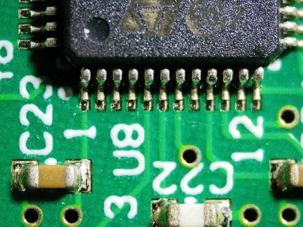
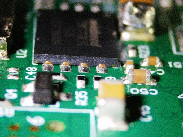
2D microscopy allows for an initial detailed inspection of components and solder joints. It is used to quickly identify:
- Solder defects (wetting issues, cracks, bridge)
- Misalignment of components
- Signs of tampering or handling
This step often serves as the starting point for the investigation
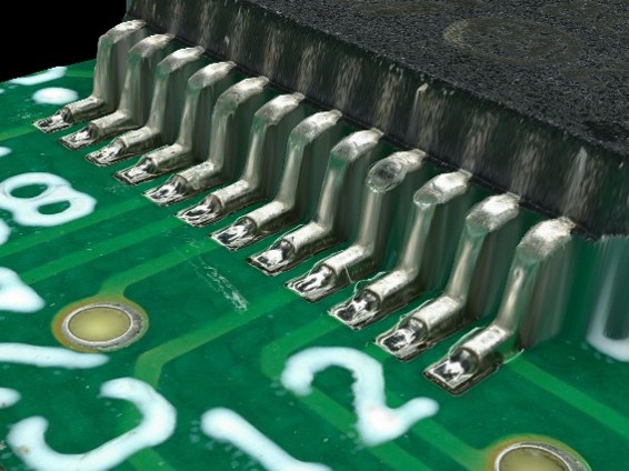
2. Topography Analysis - 3D Microscopy
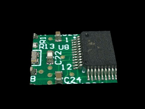
3D microscopy provides insight into volume and geometry:
- Weld profiles
- Wetting quality
- Deformations or irregularities
It also makes it possible to detect subtle clues, such as traces of rework or temporary connections (e.g., test cables), which can guide the analysis.
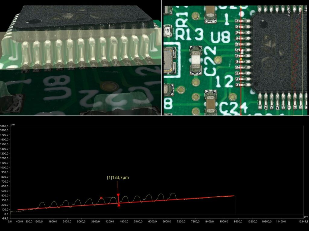
3. Measurement and Quantification
Beyond observation, it is often necessary to measure:
- Weld height and thickness
- Variations between different connections
- Surface profiles
This quantitative data makes it possible to validate hypotheses and reduce uncertainty in the diagnosis.
4. Internal Inspection — X-rays
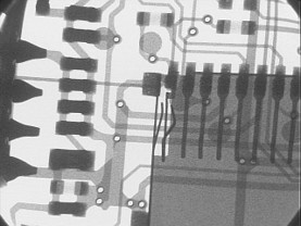
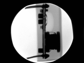
X-rays allow us to visualize internal structures without damaging the circuit:
- Hidden solder joints (BGA, QFN, etc.)
- Internal interconnections
- Component placement
This technique is essential when defects are not accessible from the surface.
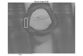
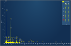
5. Materials Analysis — Electron Microscopy (SEM / EDS)
In some cases, geometric observation alone is not sufficient. It is necessary to precisely identify the nature of the materials involved in a failure.
Electron microscopy, combined with elemental analysis (EDS), allows us to:
- Observe defects at very high resolution
- Identify the chemical composition of materials
- Analyze corrosion or oxidation phenomena
This approach is particularly useful for investigating:
- Weld defects related to contamination
- Wetting or adhesion issues
- Environmental degradation
- The presence of unexpected materials
6. Physical Analysis — Cross-Section
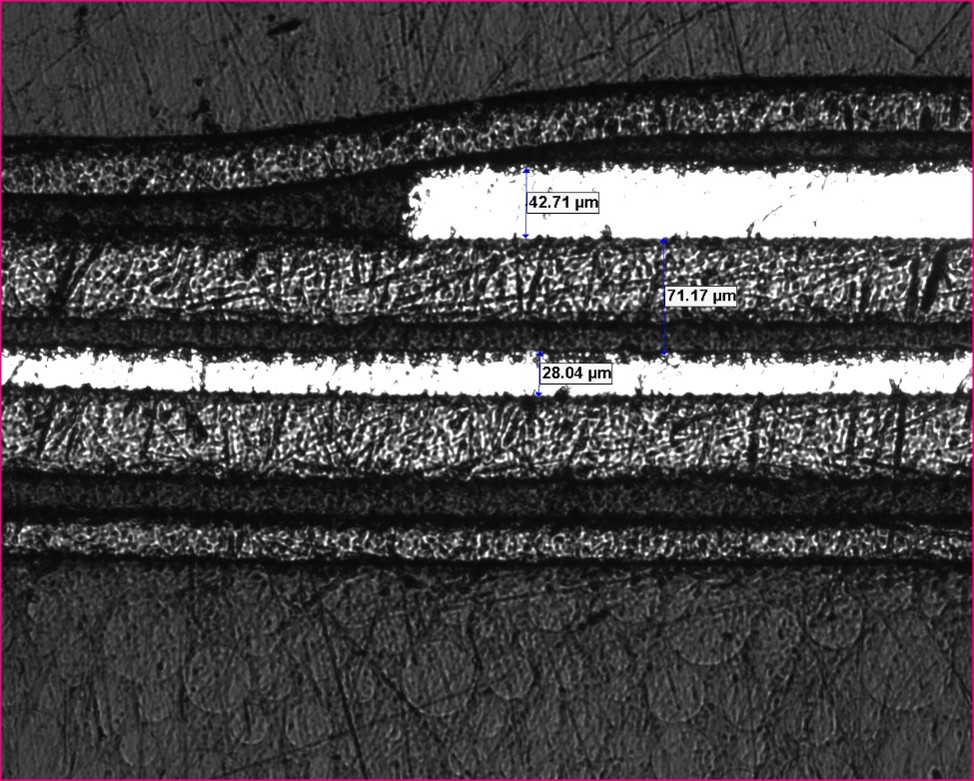
When necessary, a cross-section of the printed circuit board allows for a detailed physical analysis:
- Validation of the layer stackup
- Measurement of conductor and insulator thicknesses
- Assessment of material quality
This approach provides direct, measurable evidence of manufacturing or design deviations.
Vue de coupe d’un PCB flexible
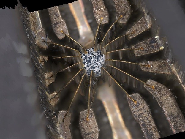
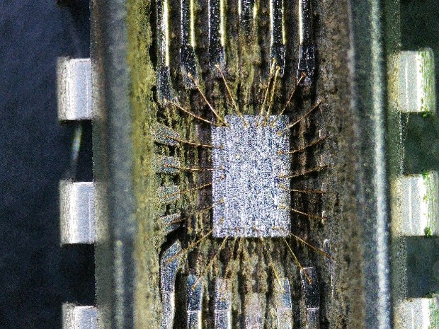
7. Laser Decapsulation of Integrated Circuits
When necessary, Novika can perform laser decapsulation of an integrated circuit:
- Verification of the defective area
- Precise identification of the pin responsible for causing the defect.
This method allows direct access to the core of the integrated circuit or its components.
From Observation to Understanding
Each technique provides a piece of the information. It is their combination that makes it possible to:
- Identify root causes
- Validate or invalidate hypotheses
- Understand the interactions between design, manufacturing, and use
At Solutions Novika, we don’t just look at the symptoms:
we seek to understand and explain why a circuit isn’t working as expected.
Real-World Example: When Stackup Affects Signal Integrity
During one production run, an electronic card containing DDR memory and a microprocessor had a production rejection rate of 8 to 10%.
The symptoms observed were :
- Intermittent behavior
- Memory link instability
- No obvious defects detected during standard inspection
A cross-sectional analysis of the printed circuit board revealed a critical defect:
➡️ The actual stackup did not meet the design specifications.
Variations in the thickness of the dielectric layers caused a change in the impedance of the transmission lines between the memory and the microprocessor.
👉 Result :
- Impedance mismatch
- Deterioration of signal integrity
- Erreurs difficiles à détecter en test classique
Errors that are difficult to detect in conventional testing
Tangible Value for Your Projects
A thorough understanding of failures makes it possible to :
- Reduce costs associated with rework and rejects
- Prevent problems from recurring
- Accelerate product development
- Ensure the safety of electronic designs
At Novika, we primarily work in the following areas:
- Research and development (R&D)
- Investigation of in-service failures
- Validation of electronic designs
- Analysis of complex or intermittent cases
Our goal is not just to identify a problem, but to provide a clear and actionable understanding.
Because, ultimately, we are part of the solution.
Are you facing a problem that’s difficult to explain or reproduce?
Our team can help you analyze and resolve your electronics-related challenges.